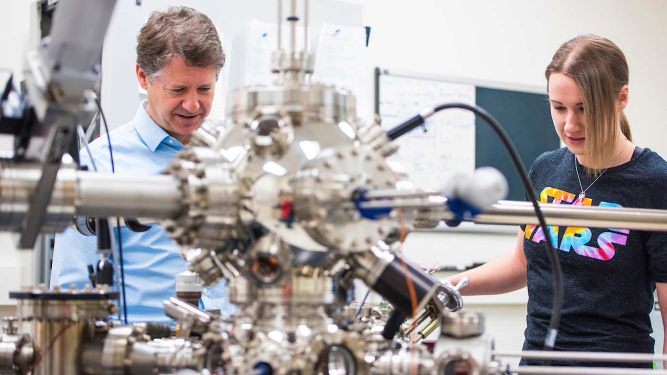
Bob Wolkow and Taleana Huff are patterning and imaging electronic circuits at the atomic level.
Imagine patterning and visualizing silicon at the atomic level, something which, if done successfully, will revolutionize the quantum and classical computing industry. A team of University of Alberta scientists has done just that, led by a world-renowned physicist and his up-and-coming protégé.
PhD student Taleana Huff teamed up with her supervisor Robert Wolkow to channel a technique called atomic force microscopy-or AFM-to pattern and image electronic circuits at the atomic level. This is the first time the powerful technique has been applied to atom-scale fabrication and imaging of a silicon surface, notoriously difficult because the act of applying the technique risks damaging the silicon. However, the reward is worth the risk, because this level of control could stimulate the revolution of the technology industry.
"It's kind of like braille," explains Huff. "You bring the atomically sharp tip really close to the sample surface to simply feel the atoms by using the forces that naturally exist among all materials."
"Imagine instead of your phone battery lasting a day that it could last weeks at a time, because you're only using a couple of electrons per computational pattern." -Taleana Huff
One of the problems with working at the atomic scale is the risk of perturbing the thing you are measuring by the act of measuring it. Huff, Wolkow, and their research collaborators have largely overcome those problems and as a result can now build by moving individual atoms around: most importantly, those atomically defined structures result in a new level of control over single electrons.
This is the first time that the powerful AFM technique has been shown to see not only the silicon atoms but also the electronic bonds between those atoms. Central to the technique is a powerful new computational approach that analyzes and verifies the identity of the atoms and bonds seen in the images. "We couldn't have performed these new and demanding computations without the support of Compute Canada. This combined computation and measurement approach succeeds in creating a foundation for a whole new generation of both classical and quantum computing architectures," says Wolkow.
Ultra-fast, ultra-low-power technology
He has his long-term sights set on making ultra-fast and ultra-low-power silicon-based circuits, potentially consuming one thousand times less power than what is currently on the market.
"Imagine instead of your phone battery lasting a day that it could last weeks at a time, because you're only using a couple of electrons per computational pattern," says Huff, who explains that the precision of the work will allow the group and potential industry investors to geometrically pattern atoms to make just about any kind of logic structure imaginable.This hands-on work was exactly what drew the self-described Canadian-by-birth American-by-personality to condensed matter physics in the University of Alberta's Faculty of Science. Following undergraduate work in astrophysics-and an internship at NASA-Huff felt the urge to get more tangible with her graduate work. (With hobbies that include power lifting and motorcycle restoration, she comes by the desire for tangibility quite honestly.) "I wanted something that I could touch, something that was going to be a physical product I could work with right away," says Huff.
And in terms of who she wanted to work with, she went straight to the top, seeking out Wolkow, renowned the world over for his work with quantum dots, dangling bonds, and industry-pushing work on atomic-scale science. "He just has such passion and conviction for what he does," she continues. "With Bob, it's like, 'we're going to change the world.' I find that really inspiring," says Huff.
"Taleana has the passion and the drive to get very challenging things done. She now has understanding and skills that are truly unique in the world giving us a great advantage in the field," says Wolkow. "We just need to work on her taste in music," he adds with a laugh.
The group's latest research findings, "Possible observation of chemical bond contrast in AFM images of a hydrogen terminated silicon surface" were published in the February 13, 2017 issue of Nature Communications. (DOI: 10.1038/NCOMMS14222)
An animation illustrating patterning and imagining electronic circuits at the atomic level. It shows the tip and surface atoms' relaxation during DFTB calculations of a part of the image simulation at small tip-surface distance. The bending and rotation of bonds is visible giving a sense of the interactions and atomic relaxations involved. (Courtesy Wolkow Lab.)